Publication History
Submitted: November 18, 2023
Accepted: November 27, 2023
Published: December 11, 2023
Identification
D-0169
Citation
Rakin Hossain Rayean & Narayan Chandra Nath (2023). Design of Solar Cell with Comparative Analysis on Different Parameter Using PSpice. Dinkum Journal of Natural & Scientific Innovations, 2(12):750-764.
Copyright
© 2023 DJNSI. All rights reserved
750-764
Design of Solar Cell with Comparative Analysis on Different Parameter Using PSpiceOriginal Article
Rakin Hossain Rayean 1*, Narayan Chandra Nath 2
- Department of Electrical & Electronic Engineering University of Information technology & Sciences Dhaka-1217, Bangladesh; rakin.hossain01921@gmail.com
- Department of Electrical & Electronic Engineering University of Information technology & Sciences Dhaka-1212, Bangladesh; ncn.uits@gmail.com
* Correspondence: rakin.hossain01921@gmail.com
Abstract: The current study was based on the research about the implementation of Photovoltaic model in PSpice. The analysis is extended into a complete characteristic of a photovoltaic module. The analysis begins with the study of the circuitry formation and thus, constructing the model of solar cell using PSpice with the graphical analysis. The effect of the current density and characterization with different diode in a photovoltaic module are discussed. In this study –two experiments, density phenomenon and diode characteristics are conducted. The formulations of the experimental result with simulation are also discussed. Hence, this showed that the both criteria and result and analysis proved that the module that represented is valid. Last but not least, an implementable solar characteristic is successfully developed.
Keywords: solar cells, photovoltaic cells, parameters
- INTRODUCTION
Photovoltaic is a generalized term used to describe the introduce of potential difference that caused electricity by generating photon that converts the light as an energy to directly producing electricity using solar cell. The term “Photovoltaic” comes from Greek word meaning light and volt from the aspiration of potential difference invented by Alessandro Volta, commonly known as voltage. It is a method that works under the phenomenon known as photovoltaic effect [1]. The voltage that generated in the solar cell is caused by the light generated carries by the p-n junction causes a movement of electrons to the N type side and hole to the P type side of the junction. Thus a p-n junction is formed which caused the solar cell to operate. A photovoltaic system is modular system found in Megawatt to mili-watt range producing electricity from power station to wrist watch [2]. In the period after the World War II much effort was put into the reconstruction of the Society. The emphasis was directed on the growth and efficiency of the mass production. New technologies and new materials, such as plastic, were applied in the production [3]. The energy demand was tremendously growing in this period. Oil and gas started to play an important role as energy sources in the second half of the 20th century. Coal, oil, and gas form today dominant sources of energy. These three energy sources, also known as fossil fuels, are called the traditional energy sources. In this period nuclear energy was introduced as a new source of energy. Increasing and more efficient mass production resulted in the low price of many household products. The consumption of the products grew enormously and therefore it is not surprising that we characterize today society as a consumption society [4, 5]. Photovoltaic system-commonly known as PV system has become an outstanding achievement in this energy striking Common Era of modern civilization in the field of electricity production and implementation. It is considered to deliberate improvement of this industry in the way of PV module array consisting of solar cell that working principle solely depends upon P-N junction characteristics. Since the solar system has an outstanding probability to lead the power and electronics field in the near future, the crying need of attaining a solar model with nearest theoretically approved is being considered a step ahead to practically implementable solar characteristics is the prime goal that cover this whole project. The Simulation program can be divided into three categories- Firstly, the simulation model is presented with parameters determined –Secondly, a circuit model is established that resemble the output to create the picture of solar cell electrical feature and module-and finally the simulation result that caused by different parameters evaluated through comparison with experimental data. This study is also influenced by varying isolation with or without different diode model to obtain different I-V characteristics and also temperature effects. This paper is also described the comparison within the implementable of this practical model than that of ideal theoretical characteristics. The performance is based on worldwide acceptable normally evaluated under the Standard test spectrum (STC)-which has been considered as average solar spectrum AM1.5 G, at an irradiance of 1000W/m2 , that give approximately 970 W/m2. It is obvious that AM1.5 G is the spectrum that G stands for global and both direct and diffuse radiation and also indirect radiation. Consequently this study can be described as development of Photovoltaic cell with non-uniform irradiance effect based two diode by using different diode models using PSpice simulator under the Orcad design and implementation.
- MATERIALS AND METHODS
2.1 PSpice
PSpice means Personal simulation program for integrated circuit emphasis. It is a circuit design and analyzing software that enrich the user to implement the circuit with different parameters model and having the output in different graphical form. It requires method for evaluating circuit performances and can be desired model easily implemented by using parametric text file and component modeling along with Orcad capture that derive the different characteristics to obtain the eligible outcome. Besides using the default component in PSpice, the characteristics component can be changed by changing the value of PSpice component in different model. Probe is a different program that allows the user to analyze the waveform of different parameters.
2.2 Orcad capture
Orcad capture along with PSpice gives the utilities to design the circuit in schematic diagram and implement different types of PSpice circuit model into Capture.opj format. One of the outstanding features of Orcad capture is that it’s gives the user to define a desired model that allows the user to import the desired model from PSpice using desirable parameters. In this project we used Orcad capture version 16.6.0.
2.3 Origin 8.5
Origin 8.5 is a graphing tool that allows the user to draw and manipulate the graph as desired. To merge the all graph output we used in this project.
3.4 Research steps
- Define the *.lib file in PSpice
- Define the circuit *.cir file in PSpice.
- Make exportable to Orcad capture by making .olb file of library file
- Implement the library in Orcad capture
- Draw the circuit
- Find the output using different markers from Orcad
- Changing in different parameters
- Save the output in*.csv format
- Accumulate all the output graphical waveform (i.e. I-V characteristic,
- Temperature ….)
- Establishing the explanation of experimental output.
- FINDINGS AND DISCUSSIONS
3.1 System Parameters
- a) Current Density
According to the theory of electromagnetism – ‘The current density is the electric current per unit area of cross section’. It is defined as a vector whose magnitude is the electric current per cross-sectional area at a given point in space (i.e. it is a vector field). In SI units, the electric current density is measured in amperes per square meter. Circuit performance depends strongly upon the designed current level, and the current density then is determined by the dimensions of the conducting elements. For example, as integrated circuits are reduced in size, despite the lower current demanded by smaller devices, there is trend toward higher current densities to achieve higher device numbers in ever smaller chip areas. High current densities have undesirable consequences. Most electrical conductors have a finite, positive resistance, making them dissipate power in the form of heat. The current density must be kept sufficiently low to prevent the conductor from melting or burning up, the insulating material failing, or the desired electrical properties changing. At high current densities the material forming the interconnections actually moves, a phenomenon called electro-migration. In superconductors excessive current density may generate a strong enough magnetic field to cause spontaneous loss of the superconductive property.
- b) Fermi-energy distribution condition due to current density
The current density that flows out of the solar cell at zero bias is named the short-circuit current density Jsc. On the other hand, the current density that flows out of the solar cell at maximum bias condition is named the open-circuit current density Jo .When a semiconductor is illuminated additional electrons and holes are generated in the material by the absorption of photons. The photo-generated carriers interact with the semiconductor lattice. The extra energy that the electron-hole pairs receive from the photons that have energy larger than the band gap of the semiconductor is released into the lattice in form of heat. After this so called thermalization process, which is very fast and takes approximately 10-12 s, the carrier concentrations achieve a steady-state. In non-equilibrium states two Fermi distributions are used to describe the electron and hole concentrations. One Fermi distribution with the quasi-Fermi energy for electrons, EFC, describes the occupation of states in the conduction band with electrons. Another Fermi distribution with the quasi-Fermi energy for holes, EFV, describes the occupation of states in the valence band with electrons, and therefore determines also the concentration of holes. The difference between the quasi- Fermi levels is the electrochemical energy- 𝜇𝑒ℎ, of the generated electron-hole pairs which represents the measure for the conversion efficiency of solar radiation. The density of electrons and holes under non-equilibrium conditions is described by-

It follows by non-equillibrium conditions.

By using the quasi-Fermi level formalism for describing the concentration of charge carriers in non-equilibrium conditions the electron and hole current densities inside a semiconductor, JN and JP, can be expressed by following equations:

When a quasi-Fermi level varies with position the current is flowing inside the semiconductor. By checking the position dependence of the quasi-Fermi levels in an energy band diagram, one can easily determine whether current flows inside the semiconductor. Drift, diffusion, and recombination-generation processes give rise to a change in the carrier concentrations in time. Nevertheless, there must be a spatial and time continuity in the carrier concentrations. Drift is charged-particle motion in response to an electric field. In an electric field the force acts on the charged particles in a semiconductor, which accelerates the positively charged holes in the direction of the electric field and the negatively charged electrons in the direction opposite to the electric field. The electron and hole drift-current densities are defined by Equation and the total drift current by

When carriers (electrons and holes) are moved due to an electric field, we call this drift. If we have a field from a positive source to a negative, the electrons in the conduction band will move towards the positive source, while the holes in the conduction band will move towards the negative. But since the holes are just the absence of a valence electron, this means that what really happens is that electrons in the valence band also move in the direction of the positive field, and they both contribute to the current. Diffusion is a process whereby particles tend to spread out from regions of high particle concentration into regions of low particle concentration as a result of random thermal motion. A gradient in concentration of particles in a semiconductor is the driving force for the transport of particles associated with diffusion. Currents resulting from diffusion are proportional to the gradient in particle concentration and the total diffusion current by the following Equation. The total current due to both drift and diffusion is expressed by
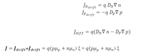
The constants of proportionality, DN and DP, are referred to as electron and hole diffusion coefficients, respectively. The electron and hole current densities inside a semiconductor, JN and JP, are obtained by adding the current densities due to drift and diffusion.

The whole processes is summarized in this way-
- When light is incident on a solar cell, carriers get generated at that surface, but not in the bulk of the solar cell. This creates a carrier concentration gradient within the semiconductor. 2. When a carrier concentration gradient exists in the semiconductor, through random motion, carriers will have a net movement from areas of high carrier concentration to areas of low concentration in the process of diffusion. 3. With time, these carriers will diffuse throughout the cell until the concentration is uniform. In summary- Diffusion refers to the phenomena where electrons or holes distribute themselves more evenly if they are initially unevenly distributed. If there is an area in a semiconductor crystal lattice where there are a lot of electrons and holes, these will both move in the directions of less concentration. Then both electrons and holes move in the same direction, and this means that the electrons in the valence band and the electrons in the conduction band move in opposite directions. If there is just as many holes and electrons moving from one place to another, then the currents will cancel each other out, and there will be no net current.
3.2 Experimental analysis of proposed solar cell according to density phenomenon
Now we are going to analyze in an abstract phrenology under the different condition of current density. Here we are going to cover the phenomenon under parametric analysis with different condition for obtaining the output. Area: The area is denoted as how much the graph is covered in the specific boundary condition. Here we hold the area in constant so that we can analyze the current density in a specific proportion. This area actually covered the whole current density condition under different circumstances. Open circuit current density (J0): The current density that flows out of the solar cell at maximum bias condition is known as the open circuit current density. Short circuit current density (Jsc): The current density that flows out of the solar cell at zero bias condition is known as the short circuit current density.

Figure 01: Voltage bias condition due to current density causing by irradiance
Circuit analysis: We’re fix the area with the open circuit current density (J0) condition while varying the short circuit condition of current density (Jsc). Each time the current density changes, the output are dramatically changes with those specific properties.
Area =126.6 j0=1e-11 jsc=0.0343
Area =126.6 j0=1e-11 jsc=0.0543
Area=126.6 j0=1e-11 jsc=0.0743
Model library:
*************************************** *
* CELL_1.CIR *
****************************************
.include cell_1.lib
xcell1 0 31 32 cell_1 params: area=126.6 j0=1e-11 jsc=0.0343/0.0543/0.0743
vbias 31 0 dc 0
virrad 32 0 dc 1000
.plot dc i(vbias)
.probe
.dc vbias -0.1 0.6 0.01
.end
Fill factor: The short-circuit current and the open-circuit voltage are the maximum current and voltage respectively from a solar cell. However, at both of these operating points, the power from the solar cell is zero. The “fill factor”, more commonly known by its abbreviation “FF”, is a parameter which, in conjunction with Voc and Isc , determines the maximum power from a solar cell. The FF is defined as the ratio of the maximum power from the solar cell to the product of Voc and Isc.
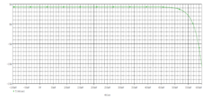
Figure 2: I-V at Jsc 0.0343 condition
From the graph it has been pointed out that the three characteristic type of curve are overlap with a quite distance with each other. According to the nature of the graph – we have to consider the condition of Fill factor for having the output explanation. It has been pictured that the green curve is dramatically slope between all other curved with the correspondent highest fill factor among the three curve. Thus due to current density consideration the green curve causing more power output with its respective current density 0.0743. The next candidate could be described of the red curve with a highest peak among the others. This curve possesses the current density with an amount of 0.0543. Naturally the logical sequence is the black curve with a current density of 0.0343 with an amount of fill factor 0.81731. This observation also demands that the fill factor is increase with the increase in current density. Therefore it can be said that fill factor is proportional to the increase in current density. Solar cell resistance parametrically response in a drastically exchange due to current density. Here we consider the shunt resistance within a range of value 100000. The series resistances are fixed within a range of parameter. Since we have found experimentally 0.0743 is the most acceptable value according to fill factor we have imposed it within a shunt resistance. Since we have found experimentally 0.0743 is the most acceptable value according to fill factor we have imposed it within a shunt resistance. Here since the current density is fixed for our highest acceptable value thus the nature of the graphical analysis is given below-
| Rs parameter | ||||
| 0.0001 | 0.001 | 0.01 | 0.1 | 1.0 |
Model library
****************************************
*CELL_2.CIR *
****************************************
.include cell_2.lib
xcell2 0 31 32 cell_2 params:area=126.6 j0=1e-11 j02=1E-9
+ jsc=0.0343 rs={RS} rsh=100000
.param RS=1 vbias 31 0 dc 0
virrad 32 0 dc 1000
.plot dc i(vbias)
.dc vbias -0.1 0.6 0.01
.step param RS list 0.0001/0.001/0.01/0.1/1.0
.probe
.end
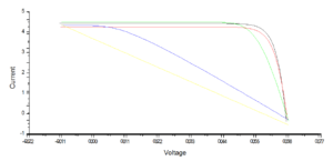
Figure 03: Comparison of resistance under Rs=0.0001, 0.001, 0.01, 0.1, 1
The Solar cell Model for I-V characteristics

Figure 04: Basic model (effect of AM1.5G without diode)
Figure 4 shows a solar model based on STC (standard test condition) of AM1.5G depicted as U1 in which the irradiance is normalized to 1000W/m2 and the cell temperature is defined as 25O C.
The value of spectral irradiance is given by (1)-
- NODES
- (11) spectral irradiance in (W/m2micron)
- (12) reference
| .subckt AM15G 11 10
v_am15g 11 10 pwl + 0.295u 0 + 0.305u 9.2 + 0.315u 103.9 + 0.325u 237.9 + 0.335u 376 + 0.345u 423 + 0.350u 466.2 + 0.360u 501.4 + 0.370u 642.1 + 0.380u 686.7 + 0.390u 694.6 + 0.400u 976.4 + 0.410u 1116.2 + 0.420u 1141.1 + 0.430u 1033 + 0.440u 1254.8 + 0.450u 1470.7 + 0.460u 1541.6 + 0.470u 1523.7 + 0.480u 1569.3 + 0.490u 1483.4 + 0.500u 1492.6 + 0.510u 1529 + 0.520u 1431 + 0.530u 1515.4 + 0.540u 1494.5 |
+ 0.550u 1504.9
+ 0.570u 1447.1 + 0.590u 1344.9 + 0.610u 1431.5 + 0.630u 1382.1 + 0.650u 1368.4 + 0.670u 1341.8 + 0.690u 1089 + 0.710u 1269.0 + 0.718u 973.7 + 0.724u 1005.4 + 0.740u 1167.3 + 0.753u 1150.6 + 0.758u 1132.9 + 0.763u 619.8 + 0.768u 993.3 + 0.780u 1090.1 + 0.8u 1042.4 + 0.816u 818.4 + 0.824u 765.5 + 0.832u 883.2 + 0.84u 925.1 + 0.86u 943.4 + 0.88u 899.4 + 0.905u 721.4 + 0.915u 643.3 + 0.925u 665.3 + 0.93u 389 + 0.937u 248.9 |
+ 0.948u 302.2
+ 0.965u 507.7 + 0.980u 623 + 0.994u 719.7 + 1.040u 665.5 + 1.070u 614.4 + 1.1u 397.6 + 1.12u 98.1 + 1.13u 182.2 + 1.137u 127.4 + 1.161u 326.7 + 1.18u 443.3 + 1.2u 408.2 + 1.235u 463.1 + 1.290u 398.1 + 1.32u 241.1 + 1.35u 31.3 + 1.395u 1.5 + 1.443u 53.7 + 1.463u 101.3 + 1.477u 101.7 + 1.497u 167.1 + 1.52u 253.1 + 1.539u 264.3 + 1.558u 265 + 1.578u 235.7 + 1.592u 238.4 + 1.61u 220.4 + 1.63u 2.35.6 + 1.646u 226.3 + 1.678u 212.5 + 1.740u 165.3 |
+ 1.8u 29.2
+ 1.86u 1.9 + 1.92u 1.2 + 1.96u 20.4 + 1.985u 87.8 + 2.005u 25.8 + 2.035u 95.9 + 2.065u 58.2 + 2.1u 85.9 + 2.148u 79.2 + 2.198u 68.9 + 2.27u 67.7 + 2.36u 59.8 + 2.45u 20.4 + 2.494u 17.8 + 2.537u 3.1 + 2.941u 4.2 + 2.973u 7.3 + 3.005u 6.3 + 3.056u 3.1 + 3.132u 5.2 + 3.156u 18.7 + 3.204u 1.3 + 3.245u 3.1 + 3.317u 12.6 + 3.344u 3.1 + 3.45u 12.8 + 3.573u 11.5 + 3.765u 9.4 + 4.045u 7.2 .ends AM15G |
(1)
- 5G 37tilt angle, global spectral irradiance
- (modified trapezoidal integration)
- Total irradiance 962.5W/m2
From Hulstrom, R., Bird, R., Riordan,C., Solar Cells, vol. 15, pp. 365-391, (1985). According to the solar cell parameters the voltage is considered as the wavelength and the current in spectral irradiance. The diode models we used in this derivation are:
1-D1N3940
2-D1N4002
3-D1N3940+D1N3940
4-D1N4002+D1N4002
5-D1N3940+D1N4002
Effect of irradiance on I–V behavior for different diode due to piecewise linear source
For single diode the configuration could be

Figure 05: Single Diode configurations

Figure 06: Double Diode configurations
The marker depicted in the figure is a current marker that paves the way to gain the I-V output of this specific solar cell condition. The parameters that used in DC sweep for Voltage V1 is given by-

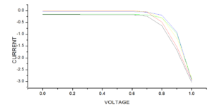
Figure 07: Characteristics of solar cell using different diodes model
Figure 7 shows the output of proposed solar cell. Here all define diode characteristic is compared. Please be noted that all diode working condition voltage source is within 1V. Since we considered the wavelength as voltage source, the graph characteristic is also as per defined. The surprising factor of the graph characteristics indicate that all diode model considered to reach their final point 1V with a reduction of graph that arc meet from the different peak of current as considered spectral irradiance. The nature of data AM1.5G spectrum paves the way that dramatically reaches the point approximately 1V. The other remarkable feature of this graph claimed that all the current that formed are nearly fluctuated at the negative magnitude. Also the plateau of 0.7V of all curves indicates that the silicon based solar cell characteristics is nearly obtained. According to the nature of graph, the more credibility obtained of this model is Red curve that inherit the highest peak of voltage so sharply. So this case analysis we consider the red curve as basic. The next candidate to obtain the credibility is Black curve that indicates a slight different in current than that of Red curve but the voltage in obtained so sharply. Therefore the Black curve represent the lower irradiance as per fill factor and so the power produced by this may be eventually considered. The yellow curve is reduced further than that of black curve. Thus the nature of curve suggest that the minority carrier transport phenomenon of electronic theory pave the way to increase the current but with through negative with respect to the nature of AM1.5G spectrum. The outcome of voltage nature is slightly obtained to maximum open circuit voltage.
Temperature characteristics
One of the important factors that need to consider is the characteristics of diode in different temperature. The optimum temperature of solar cell is 250 C. The effect of varying temperature on PV cell affect the short circuit current Isc and also change the diode saturation current Is. Like all other semiconductor devices, solar cells are sensitive to temperature. Increases in temperature reduce the band gap of a semiconductor, thereby effecting most of the semiconductor material parameters. The decrease in the band gap of a semiconductor with increasing temperature can be viewed as increasing the energy of the electrons in the material. Lower energy is therefore needed to break the bond. In the bond model of a semiconductor band gap, reduction in the bond energy also reduces the band gap. Therefore increasing the temperature reduces the band gap. In a solar cell, the parameter most affected by an increase in temperature is the open-circuit voltage. For temperature affect the PV equation of solar cell is-
![]()
The reason that varying the temperature that affected is the partial shading. Soft shades are where the sun’s rays are scattered and becomes diffuse which can be cause by little dense clouds or dirt. On the other hand, the hard shadowing is when the sun’s rays are complete disrupted, and not reaching the surface of the module. The temperature output of given diode is approximately similar. Thus we will analysis a double diode condition of proposed solar cell.
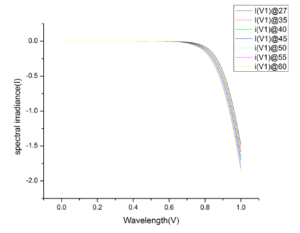
Figure 08: Temperature sweep analysis (effect of temperature in proposed cell)
We know from solar cell theory is that the semiconductor is negative temperature coefficient. From the figure it has been said that with the reduction of spectral irradiance, the wavelength is deliberately increased with the decreased in temperature. So our diode model is eventually practicable. Solar PV panels are like semiconductor devices, which are sensitive to temperature. Variation of temperature causes reduces the band gap of semiconductor devices and effects the parameters of semiconductor material. In a solar PV, mostly open-circuit voltage (VOC), short circuit current (ISC) and saturation current (IS) are affected by variation of Temperature.
Proposed solar model in array mode
The performance of a solar PV array is dependent on the operation conditions and field factor, such as sun’s geometric location, radiation level and also ambient temperature. The performance of the array depends on the behavior of each individual solar cell where the performance of each solar cell module is available in the data sheet provided. When a cell is shaded, this cell behaves as a load, taking current from other cells instead of generating its own, thus leading to a decrease in array output.
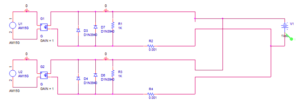
Figure 09: Proposed solar cell to form array (by diode D1N3940)
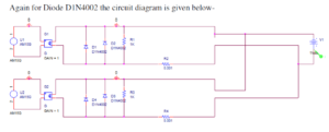
Figure 10 Proposed solar cell to form array (by diode D1N4002)
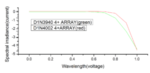
Figure 11: I-V characteristics with array model of proposed solar cell
It has been found that we could reach some clear decision according to analysis that the three characteristic type of curve are overlap with a quite distance with each other. According to the nature of the graph we decided in the way by fill factor. The current density at short circuit condition is taken into analyze with a constant in area of 126.6 and the open circuit density is also remain constant. From the theory we know that current density for a specific device should be moderated- means high excessive current density caused the device to completely damage. On the other hand much lower current density cause the device to slow for operates. Thus the green curve is the most credible candidate among the others curve with respect to their own characteristic. Though red curve seems to produce more power, the voltage tends towards more lower than green curve –with an increasing considerable amount of current- which causes more heat production than that of green curve. The black curve, on the other hand gives low voltage output moderately with respect to its current density. This observation also demands that the fill factor is increase with an increase in current density. Therefore it can be said that fill factor is proportional to the increase in current density. Again, in nested analysis of resistance according to the graph it has been said that the current density is decreases with the increase in resistance. The diode of different model is the main reason to give the scope of comparison to obtain different I-V characteristics. The diode formation in the circuit results in different I-V character in different graph. According to article 5.4 explanation, since the Red curve is far better in obtaining the nearest applicable characteristics between all diodes, we can say that the diode that creates the red curve i.e. D1N3940+D1N3940 (RED) is suited with the proposed model better than other diodes. The other curve black, green, blue and yellow also obtained with their respective characteristics. Since the red curve accomplished the nearest condition theoretically, we therefore, has the red curve as reference curve. Since our target to get the more output with lowest irradiance, it has been said that the black curve represent the diode i.e. D1N3940 is suitable with this circuit model. Therefore we can say that point 3 is supported the double diode model and point 6 is supported for single diode model as a better candidate to applicable the proposed solar model. The negative spectral irradiance i.e. current specify that we are having reduced current characteristic due to minority carrier for the using data of AM1.5G. In temperature analysis we have done the analysis in a parametric frame. Since the semiconductor is negative temperature coefficient, it has been said that with the reduction of spectral irradiance, the wavelength is deliberately increased with the decreased in temperature. So our diode model is eventually practicable. The array model is further suggested that this model could be implemented practically as the proposed theoretical solar cell is established. The array model output demand that the red curve demand more power than that of green curve. According to the dark current phenomenon (see article 2.13) our proposed model is suited for our given diode model. The negative current could also be approved to our given diode model phenomenon. Sequential penetration of tend towards positive axes is being considered for achieving result. Therefore the diode sequences area (a) D1N4002+D1N4002 (BLUE); b) D1N4002 (GREEN); c) D1N3940+D1N4002 (YELLOW); d) D1N3940+D1N3940 (RED); e) D1N3940 (BLACK).
- CONCLUSION
The model characterizations of solar cell are successfully modeled in PSpice with varying current density and the different diode parameters. The result of the current density module is similar to the real characteristics module. The simulation result are slightly different in AM 1.5 G as well as with the real solar module. This study also shows the temperature effect of solar module with different aspects. The model library is defined and thus the prospects of solar cell characteristics are analyzed. The parameter validation and the graphical output are also performed. Last but not least this module characterization is also recommended the further improvement in the application field.
REFERENCES
- Abankwah, B., Vincent, A., & Usamah, M. (2023). A REVIEW (OF CONSTRUCTION ECONOMIC (COST MANAGEMENT BASED ON GHANA MARKET ECONOMY. History, 2(03), 144-150.
- Castolo, Caroline T., and Carmencita L. Sumande. “A review of economic cost management based on Philippine market economy.” Dinkum Journal of Economics and Managerial Innovations2, no. 06 (2023): 352-358.
- Sarkar, Md Nazmul Islam. “Effect of various model parameters on solar photovoltaic cell simulation: A SPICE analysis.” Renewables: Wind, Water, and Solar3, no. 1 (2016): 1-9.
- Dash, Soubhagya Kumar, R. Akhil Raj, Savita Nema, and R. K. Nema. “A quantitative and comparative performance evaluation of PV models on PSPICE platform.” In 2015 International Conference on Circuits, Power and Computing Technologies [ICCPCT-2015], pp. 1-8. IEEE, 2015.
- Jiang, Yuncong, Jaber A. Abu Qahouq, and Mohamed Orabi. “Matlab/Pspice hybrid simulation modeling of solar PV cell/module.” In 2011 Twenty-Sixth Annual IEEE Applied Power Electronics Conference and Exposition (APEC), pp. 1244-1250. IEEE, 2011.
- https://en.wikipedia.org/wiki/Diode#Shockley_diode_equation
- Luis castener , Santigo Silvestre –Modelling photovoltaic system using Pspice-wiley(2003)
- Hulstrom, R., Bird, R., Riordan,C., Solar Cells, vol. 15, pp. 365-391, (1985)
- www .pveducation.org
- Castaner, Luis, and Santiago Silvestre. Modelling photovoltaic systems using PSpice. John Wiley and Sons, 2002.
- Aouchiche, N., M. Becherif, A. HadjArab, M. S. Aitcheikh, H. S. Ramadan, and A. Cheknane. “Dynamic performance comparison for MPPT-PV systems using hybrid Pspice/Matlab simulation.” International Journal of Emerging Electric Power Systems17, no. 5 (2016): 529-539.
- Dash, Soubhagya Kumar, R. Akhil Raj, Savita Nema, and R. K. Nema. “Development of photovoltaic (PV) cell/module/array and non-uniform irradiance effect based on two-diode model by using PSPICE simulator.” In 2015 International Conference on Nascent Technologies in the Engineering Field (ICNTE), pp. 1-6. IEEE, 2015.
- Devasia, Archana, and Santosh K. Kurinec. “Teaching solar cell IV characteristics using SPICE.” American Journal of Physics 79, no. 12 (2011): 1232-1239.
Publication History
Submitted: November 18, 2023
Accepted: November 27, 2023
Published: December 11, 2023
Identification
D-0169
Citation
Rakin Hossain Rayean & Narayan Chandra Nath (2023). Design of Solar Cell with Comparative Analysis on Different Parameter Using PSpice. Dinkum Journal of Natural & Scientific Innovations, 2(12):750-764.
Copyright
© 2023 DJNSI. All rights reserved


